Kicad Trace Length
Pymesh is a rapid prototyping platform focused on geometry processing. Altium designer, eagle, and orcad.
Trace length calculation wrt different layer Layout KiCad.info Forums

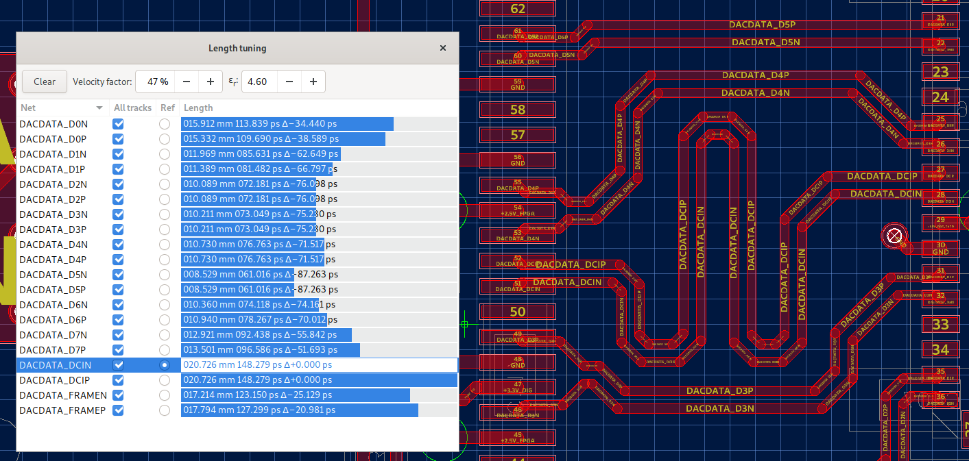
And the note now reads ‘tuned:

Kicad trace length. Check out our tutorial on how to place components in kicad. Kicad crashes when cvpcb or footprint editor opens: This latter information can be obtained from the.
That being said, there are three pcb design packages that tend to be the most popular and considered the best: Donations are accepted via credit card and purchase order (us$ That is why tuning the trace length is a critical aspect in a high speed design.
It facilitates the design and simulation of electronic hardware. Mesh3d trace is a graph object in the figure's data list with any of the named arguments or attributes listed below. The sofle rgb is a copy of the sofle v2 with the addition of up to 36 rgb leds per side.
Perhaps surprisingly, to handle 120ma we only need a trace width of 0.635 mils! Schematic creation and board layout. 39506 n daisy mountain dr.
Eeschema is a schematic capture software distributed as a part of kicad and available under the following operating systems: Kicad is a versatile tool for electronic circuit design and corresponding pcb design requiring familiarity and expertise. This guide on setting up kicad for your pcb design will help you design faster and better.
7 out of 10 there are numerous software packages available for designing printed circuit boards (pcbs), too many in fact. For this calculation, you must enter the current value of the track, the thickness of the copper, the temperatures, and finally, the length of the track. Easyeda is a free and easy to use circuit design, circuit simulator and pcb design that runs in your web browser.
In kicad there is in. Btw, there seems to be a bug in freerouting v1.4.4 as it did not stop after reaching the same # of vias and trace length for 7 times. That being said, the wider the trace the less the resistance and the more stable the supply voltage at each component.
Hence, the designer should place the resistor as close as possible to the load pin of the receiver to minimize the stub length of the connecting trace. The free, open source software allows you to create pcb layouts and schematics, and even includes a 3d viewer. The minimum width traces can be easily used for the supply lines in this design.
I = 0.048 x dt 0.44 x a 0.725 where i is maximum current in amps, k is a constant, dt is temperature rise above ambient in °c, & a is cross sectional area of trace mils². Kicad supports an integrated design workflow in which a schematic and its pcb are designed together. Seth hillbrand 9 fix committed:
It combines two or more solid shapes (say a and b ) by checking if a point x lies inside of each solid. The ability to adjust trace length matching/meandering is also planned. I = 0.024 x dt 0.44 x a 0.725 external traces:
With each trace that you create, make sure to set the width to 48 mil in the inspector on the right. Most pcb designers begin this process by grouping similar components, keeping weight distribution, trace length, and heat sinks in mind to optimize the layout of their printed. Setting grid origin in footprint library browser causes crash:
It features an integrated environment for schematic capture, pcb layout, manufacturing file viewing, spice simulation, and engineering calculation.tools exist within the package to create bill of materials, artwork, gerber. Rounder tools for tracks (to be copied on kicad plugins dir) rounder for tracks (action plugin) solder mask expander (action plugin) track length (action plugin) via fence generator (action plugin) [pyclipper required] trace clearance generator; The trace length i found, again, in kicad:.
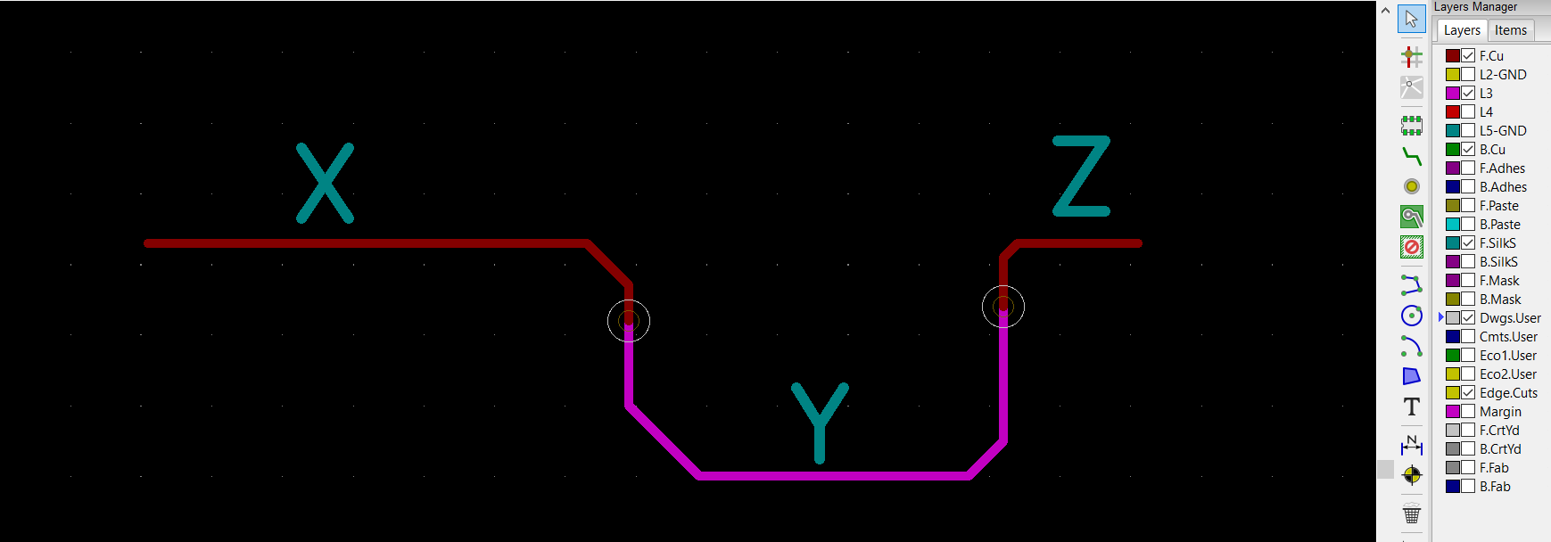
This is part of a series of short tutorials on advanced topics of using kicad, the favorite schematic/pcb design software here at wayne and layne. However, for hardware entrepreneurs, startups and makers i prefer a less. 40 mm/40 mm’, which means the length is exactly 40 mm.
It can be used on windows, linux and macos. The typical kicad workflow majorly consists of two main tasks: Generate a copper pour keepout for a selected.
Donating to kicad via the linux foundation provides funds for project development and the developers behind it. The trace thickness i found by looking up the pcb spec from osh park, who said that a two sided board uses 1 ounce copper. Cut an appropriate length from the roll using a large pair of scissors (small scissors will get stuck like a dinosaur in a tar pit!).
2 critical 9 fix committed: There is many a comment on these here pages along the lines of “why did you use a microcontroller, when you could just have easily used a. So you have two options:
As well as trying to reduce the total trace length. * use an absolute url (which will work fine for one user but may break if more than one user will be using the library) * create a kicad environment variable which points to the location of your 3d models. To accomplish these tasks, kicad includes a vast library of components and pcb footprints, and also has the tools to create new ones.
There are also no paid networks to unlock features. If it is not synchronized, the interface could fail at the maximum frequency or will not work at all. 2 critical 9 fix committed:
Higher trace lengths from the load pin to the resistor will mean that the circuit will be more susceptible to signal reflection. In kicad i make pcb board and i sent the pcb design to a chinese pcb board maker. When you use a high speed interface, you need to tune the length of the traces to synchronize signal propagation through data lines.
Design reuse will be boosted by support for layout snippets, and there will be better support for pad stacks and more. Notice in the makefile.am file that we add helloworld to the bin_programs variable. Unfortunately kicad does not support relative file paths when linking 3d models to the footprints (relative to the footprint library).
Using a value i found at pcbuniverse, a 1oz copper plane is 0.00137″ thick. With the circuit editor, you can create your design without any limitations.
Differential pair length tuning Layout KiCad.info Forums

Trace length calculation wrt different layer Layout KiCad.info Forums
Track length matching with KiCAD and FreeRouting
Die to pad length Layout KiCad.info Forums

KiCAD now with differential pair routing and trace length matching KiCad
Kicad Tune Track Length PCB Designs

Cumulative track length for a selection of tracks in pcbnew? Layout KiCad.info Forums

Kicad Track Length How to route differential pairs in KiCad Sierra Circuits In the image

Pcbway Design Rules Kicad PCB

Kicad trace length tunning test YouTube

Kicad Differential pair routing and trace length matching YouTube
Kicad Tune Track Length PCB Designs
Kicad Tune Track Length PCB Designs

Kicad Track Length How to route differential pairs in KiCad Sierra Circuits In the image

Kicad Tune Track Length PCB Designs

Multiple tracks in trace length matching Layout KiCad.info Forums

Kicad Tune Track Length PCB Designs

pcb design How can I account for package trace length in KiCAD? Electrical Engineering Stack

Trace too short, not drawn (bug?) — visible on Gerber Layout KiCad.info Forums
