Single Layer Pcb Design Software
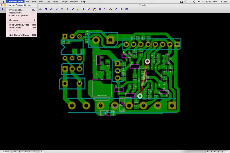
Buttons change context for schematic entry and the active bar. 3) when the pcb design file opens, the main menu bar and related.
Single layer pcb design, Printed Circuit Board Design Services, पीसीबी डिजाइनिंग सर्विस, पीसीबी
The proteus eda tools range is a professionals choice for modern printed circuit board layout.

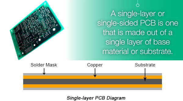
Single layer pcb design software. A planelet, a variation of a plane, is an uninterrupted area of metal covering only a portion of a pcb layer. The layer stack manager opens in a document editor in the same way as a schematic sheet, the pcb, and other document types do. • a pcb layer stack can help you minimize your circuit's vulnerability to external noise as well as minimize radiation and reduce impedance and crosstalk concerns on.
As per the pcb design perspective, the ground is separated into two parts. Our pcb prototype service is among the fastest and most reliable in the industry. You might need to use two copper layers, with traces routed on both sides of the pcb.
Billed as “the industry’s most innovative pcb design flow,” xpedition includes unique, patented technologies to reduce design cycles by at least 50% while improving overall quality and resource efficiency. Altium designer, eagle, and orcad. Pcb design cad vendor libraries:
Type the name multivibrator in the file name fieldand click save. That being said, there are three pcb design packages that tend to be the most popular and considered the best: Our customers tell us one of the reasons they love doing business with us is because of our pcb design software.
They are very important in the This is a copper layer that forms one of the layers in a pcb. Is displayed in the workspace.
We deal in the followings: Planes and planelets distribute power to a number of points on a pcb. Advanced circuits' online pcb design software is not only easy to use, it is absolutely the best free pcb layout software available!
2) to save the new pcb file, select file » save as or select save. The pcb can be a single layer and can go up to many layers as a person want, but most of the software support up to 14 layers. A leader in electronic design automation, mentor graphics pcb offers xpedition, a pcb design software tool for electronics engineers.
If you need to ensure the core circuits of a pcb design will function as intended on an assembled board, we can get one to you in as little as eight hours. This can be mapped using datasheets and formulas for generic pad shapes and sizes. Expresspcb has helped create designs to explore the bottom of the ocean, outer.
Pcb cad software expresspcb has been the free pcb layout and design software for over 20 years, used by engineers, electronic designers, students and hobbyists. Once the trace width required for specific nets to have a target impedance (usually 50 ohms) is determined, it can be set as a design rule in your pcb routing utilities. Single layer pcbs are used in applications such as calculators, power supplies, and printers.
The best pcb impedance calculator utilities inside pcb design tools will include these effects so that impedance can be determined to very high accuracy. It is a board that has lines and pads that connect various points together. Typically, a number of planelets exist in one pcb layer.
Tabulates the differences between variants of the project. The first portion is power ground and the second portion is analog or control ground. The traces on one layer can be connected to the other layer with a via.
A plane is an uninterrupted area of metal covering the entire pcb layer. Tronicszone is one of the top electronics design & manufacturing companies based out of bangalore. Includes layer stackup, drill table, fiducial data, assembly drawings and more.
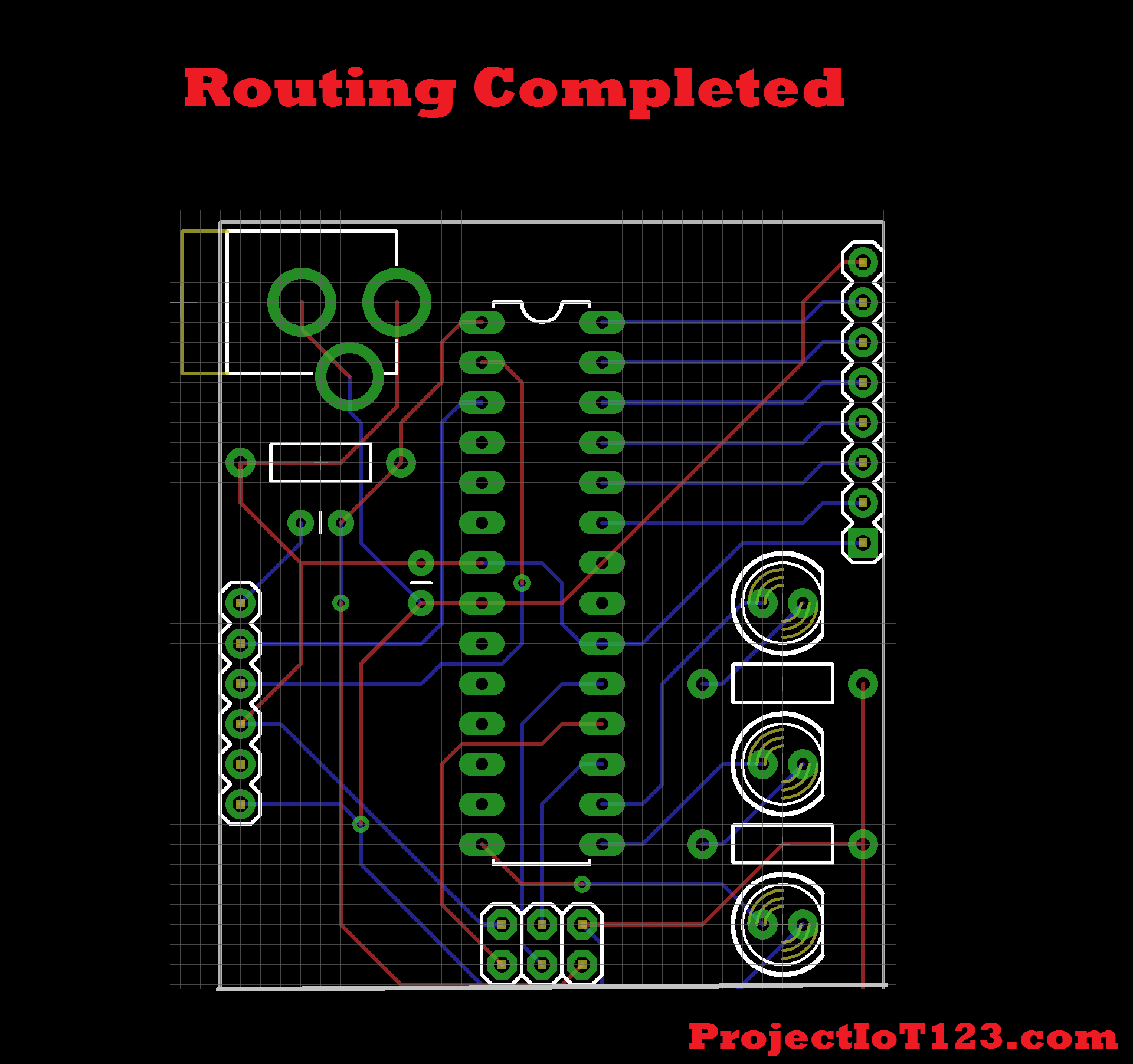
Lists in a linear table all of the design rules that have been specified for the current project. A via is a copper plated hole in the pcb that. New pcb design file in projects panel.
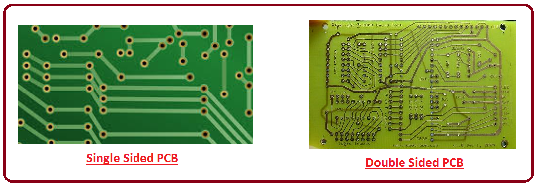
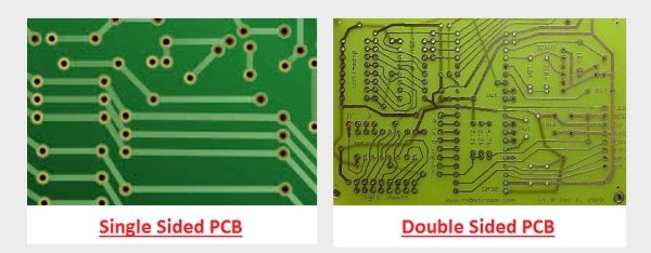
They are inexpensive to produce, and simple to design. Larger circuits can be difficult to design on a single layer pcb because it’s hard to route the traces without intersecting one another. With over 30 years of continuous development and innovation, our focus remains on adding functionality while maintaining a simple, clean user interface and tight integration with the schematic design.
Most commonly used pcb is a single sided pcb and the components and conductors on different layers of pcb. We provide a wide array of engineering services that includes, embedded systems design, custom electronics design, pcb design, iot hardware, firmware development, prototyping & electronic manufacturing services. Prototyping is a key part of a complete bespoke.
Pcb is an acronym for printed circuit board. Flex pcb, custom pcb, prototype pcb, turnkey pcb assembly, electronic pcb assembly, low volume pcb assembly etc. From the circuitry perspective, a switching power supply can have a single common ground for all components but it is not the case during the pcb design phase.
Manual design of pads involves drawing the required pad shapes using design software tools. Fits any use case— one of the major benefits of pcb design software comes from its variety of use cases. With pcb design software, users can tilt, rotate, and zoom in on their designs, providing users with a more holistic view of their board structure.
A software check of your. In this type of pcb, components are small in size because these components have very small lead or no leads are required for mounting on the board. Altium designer ® offers a unified design environment, empowering engineers with a single view of every aspect of the pcb design process from schematic, to pcb layout, to design documentation.
In typical pcb designs, various masks and surface finishes require verification of proper clearances and coverage. However, for hardware entrepreneurs, startups and makers i prefer a less. To open the layer stack manager select design » layer stack manager from the main menus.
7 out of 10 there are numerous software packages available for designing printed circuit boards (pcbs), too many in fact.
Single Layer PCB Design in Bengaluru, Indiranagar by Abisastha Technologies ID 11048553191

12 Best Free PCB Design Software in 2021
Single Layer PCB Design
Single Sided PCB The Engineering Projects
Multilayer Pcb Design In Altium PCB Circuits

Free PCB Design Software ALLPCB

eagle pcb design software tutorial projectiot123 Technology Information Website worldwide
Single Layer Pcb Design Software
2 Layer PCB Design Singapore For Electronic Circuit

High Speed Pcb Design and Layout, Expert PCB Design Service [ With Step By Step Guide]

Single Layer Pcb Design Software
What Is Single Layer PCB?

Single Layer Pcb Design Software
Free PCB Design Software ALLPCB

Single Layer PCB Design Service in Gandhinagar ID 19120278888

Single Layer PCB introduction Application and advantages

Single Sided PCB Single Layer PCB manufacturers in China

Guides for distinguishing the single layer PCB and 2 layer PCB Techno FAQ
Single Sided PCB Types of PCB Electronics & You
